MicroZed Chronicles: Clock Planning
August 19, 2022
Editor’s Note: This content is republished from the MicroZed Chronicles, with permission from the author.
When I started my design career twenty plus years ago, one of the very simple rules we had for significantly smaller and less flexible FPGAs (think XC4000XL / Virtex E/EM and Spartan) and tools was to use a single clock only whenever possible. Of course, it was not always possible but even then, the number of clocks was still limited.
Over the years, we moved to much more capable devices and tools and now we often find ourselves with complex clocking structures where we have source-synchronous devices like AXI clocks connected to processors etc., signal chain clocks, and the need to retime signals from an input clock domain to another. This is especially common in video applications.
This means we have a complex clocking environment -- one where it’s easy to get clocking wrong. This will result in timing challenges or something even worse like introducing inadvertent clock domain crossing errors which leads to corruption of the data or control follow.
We will start our journey looking at 7 Series devices. When we think about clock planning, we need to ensure that we use the most appropriate resources within the device and understand its internal clocking architecture. Long gone are the days where all we needed to do was ensure that the clock signal was connected to an appropriate clock pin on the IO.
There are two aspects to clock planning. The first comes from the architecture of the design itself and it’s here, within this architecture, where we decide how many clocks the design has and the relationships between them. Ideally, we want to perform clock domain crossing as little as possible in addition to minimizing the number of clocks used.
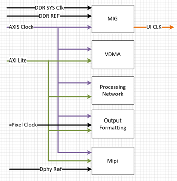
It is during this clock planning that we can draw our initial clock architecture and associated reset architecture. The clock architecture is also where we show interactions between clock domains. This is something you should be creating before you write a line of HDL or open Vivado. We can start with a simple diagram like the one below which shows the major elements and then develop it in further detail as the design develops.

Once we have the clocking architecture, we can map these clocks into the resources of the targeted device. 7 Series devices have the following range of clocking resources.
- Clock capable input pins – Single or multiple clock region capable
- Global clocks – Capable of providing clocks across an entire device
- Regional clocks – Capable of providing clocks to a clock a region (and adjacent regions)
- IO clocks – Capable of clocking IO structures
- Clock management tiles – provides advanced clocking structures such as MMCM and PLL
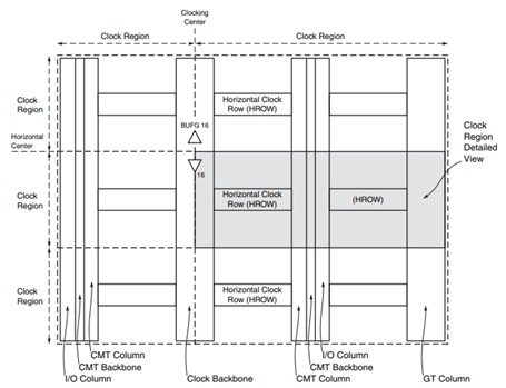
Internally, the device itself is split into several clocking regions which contain the CLBs, BRAM, DSP, GT, I/O and other features. Each region also contains several clocking resources including the ability to support the following:
- 12 global clocks
- 2 multi-region clocks
- 4 regional clocks
- 4 IO clocks
To access these, we use one of several buffer types: BUFG, BUFR, BUFIO, BUFMR. There is also a BUFH which is the horizontal clock. Global clocks are contained within the clock backbone that runs vertically and the horizontal clock provides the BUFG and BUFH to the clock region. The BUFG does not have to be within the clocking region.
Below, the diagrams show how the clock resources within a device and region are visualized quite nicely.


We can ensure the best implementation for the project with a clocking architecture and a good understanding of the resources available. This can have an impact on pin planning. One such example is if we are using DDR and MIG, we should ensure the clock input and CMT are in the same region as we implement the MIG.
Like in all designs, we need to know how the tool has implemented the design and what resources have been used.
We can use the Vivado clock report (report_clocks in the TCL window) to analyze what clocks Vivado has detected. This will show the generated defined clocks.

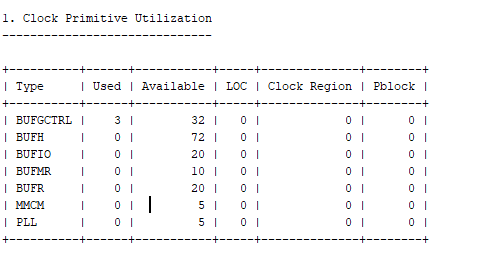
One thing we can do is run the clock utilization report (report_clock_utilization) which will show the allocation of clocks to the resources available.
The summary will provide the high-level overview of the buffer types used. In this SpaceWire design example, you can see that only a few BUFG are used within the design.

We can see the detailed usage of the global clocking resources further down the report.

This report will enable us to determine if we have implanted the clocking architecture in the manner intended for our initial architecture. If not, we can start to look at the implementation and identify where it is different.
We can run the clock interaction report and the CDC reports to help understand the issues that might be arising in the clocking network. These reports can also be used to help ensure that our constraints are correctly defined, especially when run in conjunction with the design analysis report and quality of result reports.
Xilinx Xclusive Blog
-
- AMD-赛灵思公布 2021 自适应计算挑战赛开发者赛道获胜者
- Apr 28, 2022
-
- 启动您的引擎:Versal Premium 系列引入 AI 引擎,“加速”信号处理
- Apr 20, 2022
-
- 基于自适应计算的尖端音视频与广播方案亮相 ISE 2022
- Apr 06, 2022
Adaptable Advantage 博客
-
- MicroZed Chronicles: 10 Rules for HDL Development.
- Aug 26, 2022
-
- MicroZed Chronicles: Clock Planning
- Aug 19, 2022
-
- MicroZed Chronicles: MATLAB / Simulink HDL Coder
- Aug 12, 2022