


灵活应变.万物智能.
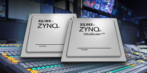
在 Xilinx,我们相信你们这些正在获得最新突破性构想的创新者、变革推动者和建设者。Xilinx 提供助您实现发明的平台。我们将帮助您更快进入市场,帮助您在不断变化的世界保持竞争力,让您始终处于行业的最前沿。
了解更多>
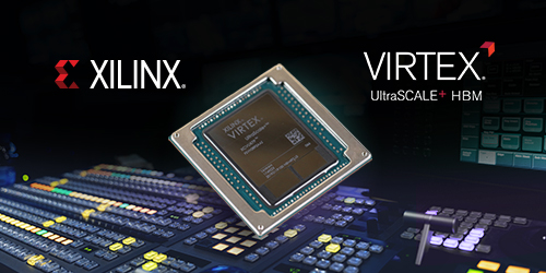
在 Xilinx,我们相信你们这些正在获得最新突破性构想的创新者、变革推动者和建设者。Xilinx 提供助您实现发明的平台。我们将帮助您更快进入市场,帮助您在不断变化的世界保持竞争力,让您始终处于行业的最前沿。
了解更多>