MicroZed Chronicles: Using DSP48E2 as Multiplexers
May 6, 2022
Editor’s Note: This content is republished from the MicroZed Chronicles, with permission from the author.
I am a regular reader of many FPGA notice boards. A few days ago, I saw a question about how the DSP48E2 could be used as a multiplexer. The question arose because the developer was running low on logic resources while the DSP elements were unused.
I had come across the Hoplite Network on Chip a few years ago and a version of this also used the DSP48 elements as multiplexers. The Hoplite-DSP version used the DSP48 as a mux to return logic resources to the FPGA designers.
The DSP48E2 is a very versatile feature. In our programmable logic, we mainly we use it to implement mathematical algorithms like filters, FFT, and so on.
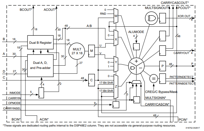
Looking at the architecture of the DSP48, however, there are several multiplexors that can be used to switch the data that is fed into the ALU.
We can multiplex a signal by controlling the setting of the X and Y multiplexor and by setting the correct mode for the ALU.
We can do this by configuring the ALU to perform an addition and selecting the input we require from the X or Y mux while setting the other mux to a constant zero. As a result, we are using the addition of 0 to the desired signal to perform the multiplexing.

We can multiplex between signals on A:B and C within the DSP48. This enables multiplexing of 48 bits of data. Of course, inputs A is 30 bits and B is 18 bits. This is combined into signal A:B after the dual A and B registers.
Signal A:B is fed into to mux X, while signal C is fed into mux Z and Y. All multiplexors W, X, Y, and Z have an input that can be selected which is all zeros.
To perform the multiplexing, we can configure the following equations using inmode, opmode, and alumode commands.
P = A:B + 0
P = C + 0
To demonstrate this, I created a simple example in Vivado using the DSP48 template from the language templates. I configured this DSP template so that I could control the opmode to switch between inputs A:B and C.
The code can be seen below. At the top level, however, the DSP mux offers the user two 48-bit ports A, C, and a select signal. Internally the A signal is routed to DSP ports A and B while port C is connected to the DSP port C.
Depending upon the state of the select signal, the op code is changed to select the correct channels on the X and Y multiplexor.
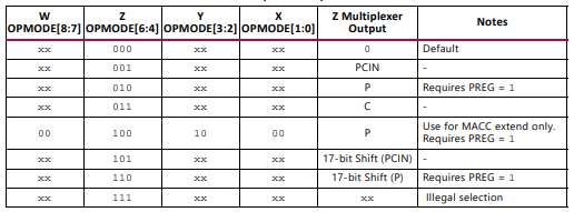
To output A:B which is connected to the X mux, we need to set OP code bits[1:0] to 11 and ensure all other multiplexors to output zero.
Similarly the same approach is taken for C which is connected to the Y mux. Its opmode[3:2] is set to 11 and all other multiplexors are set to output zero.


Library ieee;
use ieee.std_logic_1164.all;
Library UNISIM;
use UNISIM.vcomponents.all;
entity dspmux is port(
clk : in std_logic;
rst : in std_logic;
a : in std_logic_vector(47 downto 0);
c : in std_logic_vector(47 downto 0);
sel : in std_logic;
op : out std_logic_vector(47 downto 0)); end entity;
architecture rtl of dspmux is
signal ain : std_logic_vector(29 downto 0); signal bin : std_logic_vector(17 downto 0); signal cin : std_logic_vector(47 downto 0); signal ALUMODE : std_logic_vector(3 downto 0); signal INMODE : std_logic_vector (4 downto 0); signal OPMODE : std_logic_vector(8 downto 0);
begin
INMODE <= (others =>'0');
ALUMODE <= (others =>'0');
ain <= a(47 downto 18);
bin <= a(17 downto 0);
cin <= c;
process(sel)
begin
if sel = '0' then
OPMODE <= "000000011";
else
OPMODE <= "000001100";
end if;
end process;
DSP48E2_inst : DSP48E2
generic map (
-- Feature Control Attributes: Data Path Selection
AMULTSEL => "A", -- Selects A input to multiplier (A, AD)
A_INPUT => "DIRECT", -- Selects A input source,
BMULTSEL => "B", -- Selects B input to multiplier (AD, B)
B_INPUT => "DIRECT", -- Selects B input source,
PREADDINSEL => "A", -- Selects input to pre-adder (A, B)
RND => X"000000000000", -- Rounding Constant
USE_MULT => "NONE", -- Select multiplier usage
USE_SIMD => "ONE48", -- SIMD selection (FOUR12, ONE48, TWO24)
USE_WIDEXOR => "FALSE", -- Use the Wide XOR function
XORSIMD => "XOR24_48_96", -- Mode of operation for the Wide XOR
-- Pattern Detector Attributes: Pattern Detection Configuration
AUTORESET_PATDET => "NO_RESET",
AUTORESET_PRIORITY => "RESET", -- Priority of AUTORESET vs. CEP
MASK => X"3fffffffffff", -- 48-bit mask value for pattern
PATTERN => X"000000000000", -- 48-bit pattern match for
SEL_MASK => "MASK", -- C, MASK,
SEL_PATTERN => "PATTERN", -- Select pattern value
USE_PATTERN_DETECT => "NO_PATDET", -- Enable pattern detect
-- Programmable Inversion Attributes: Specifies built-in
programmable inversion on specific pins
IS_ALUMODE_INVERTED => "0000", -- Optional inversion for ALUMODE
IS_CARRYIN_INVERTED => '0', -- Optional inversion for CARRYIN
IS_CLK_INVERTED => '0', -- Optional inversion for CLK
IS_INMODE_INVERTED => "00000", -- Optional inversion for INMODE
IS_OPMODE_INVERTED => "000000000", -- Optional inversion for OPMODE
IS_RSTALLCARRYIN_INVERTED => '0', -- Optional inversion for
RSTALLCARRYIN
IS_RSTALUMODE_INVERTED => '0', -- Optional inversion for
RSTALUMODE
IS_RSTA_INVERTED => '0', -- Optional inversion for RSTA
IS_RSTB_INVERTED => '0', -- Optional inversion for RSTB
IS_RSTCTRL_INVERTED => '0', -- Optional inversion for RSTCTRL
IS_RSTC_INVERTED => '0', -- Optional inversion for RSTC
IS_RSTD_INVERTED => '0', -- Optional inversion for RSTD
IS_RSTINMODE_INVERTED => '0', -- Optional inversion for
RSTINMODE
IS_RSTM_INVERTED => '0', -- Optional inversion for RSTM
IS_RSTP_INVERTED => '0', -- Optional inversion for RSTP
-- Register Control Attributes: Pipeline Register Configuration
ACASCREG => 1, -- Number of pipeline stages(0-2)
ADREG => 1, -- Pipeline stages for pre-adder
ALUMODEREG => 1, -- Pipeline stages for ALUMODE
AREG => 1, -- Pipeline stages for A (0-2)
BCASCREG => 1, -- Number of pipeline stages(0-2)
BREG => 1, -- Pipeline stages for B (0-2)
CARRYINREG => 1, -- Pipeline stages for CARRYIN
CARRYINSELREG => 1, -- Pipeline stages for CARRYINSEL
CREG => 1, -- Pipeline stages for C (0-1)
DREG => 1, -- Pipeline stages for D (0-1)
INMODEREG => 1, -- Pipeline stages for INMODE
MREG => 1, -- Multiplier pipeline stages
OPMODEREG => 1, -- Pipeline stages for OPMODE
PREG => 1 -- Number of pipeline stages P
)
port map (
-- Cascade outputs: Cascade Ports
ACOUT => open, -- 30-bit output: A port cascade
BCOUT => open, -- 18-bit output: B cascade
CARRYCASCOUT => open, -- 1-bit output: Cascade carry
MULTSIGNOUT => open, -- 1-bit output: Multiplier sign cascade
PCOUT => open, -- 48-bit output: Cascade output
-- Control outputs: Control Inputs/Status Bits
OVERFLOW => open, -- 1-bit output: Overflow in add/acc
PATTERNBDETECT => open, -- 1-bit output: Pattern bar detect
PATTERNDETECT => open, -- 1-bit output: Pattern detect
UNDERFLOW => open, -- 1-bit output: Underflow in add/acc
-- Data outputs: Data Ports
CARRYOUT => open, -- 4-bit output: Carry
P => op, -- 48-bit output: Primary data
XOROUT => open, -- 8-bit output: XOR data
-- Cascade inputs: Cascade Ports
ACIN => (others =>'0'), -- 30-bit input: A cascade data
BCIN => (others =>'0'), -- 18-bit input: B cascade
CARRYCASCIN => '0', -- 1-bit input: Cascade carry
MULTSIGNIN => '0', -- 1-bit input: Multiplier sign cascade
PCIN => (others =>'0'), -- 48-bit input: P cascade
-- Control inputs: Control Inputs/Status Bits
ALUMODE => ALUMODE, -- 4-bit input: ALU control
CARRYINSEL => (others =>'0'), -- 3-bit input: Carry select
CLK => CLK, -- 1-bit input: Clock
INMODE => INMODE, -- 5-bit input: INMODE control
OPMODE => OPMODE, -- 9-bit input: Operation mode
-- Data inputs: Data Ports
A => AIN, -- 30-bit input: A data
B => BIN, -- 18-bit input: B data
C => CIN, -- 48-bit input: C data
CARRYIN => '0', -- 1-bit input: Carry-in
D => (others =>'0'), -- 27-bit input: D data
-- Reset/Clock Enable inputs: Reset/Clock Enable Inputs
CEA1 => '1', -- 1-bit input: Clock enable for 1st stage AREG
CEA2 => '1', -- 1-bit input: Clock enable for 2nd stage AREG
CEAD => '1', -- 1-bit input: Clock enable for ADREG
CEALUMODE => '1', -- 1-bit input: Clock enable for ALUMODE
CEB1 => '1', -- 1-bit input: Clock enable for 1st stage BREG
CEB2 => '1', -- 1-bit input: Clock enable for 2nd stage BREG
CEC => '1', -- 1-bit input: Clock enable for CREG
CECARRYIN => '1', -- 1-bit input: Clock enable for CARRYINREG
CECTRL => '1', -- 1-bit input: Clock enable for OPMODEREG and
CARRYINSELREG
CED => '1', -- 1-bit input: Clock enable for DREG
CEINMODE => '1', -- 1-bit input: Clock enable for INMODEREG
CEM => '1', -- 1-bit input: Clock enable for MREG
CEP => '1', -- 1-bit input: Clock enable for PREG
RSTA => rst, -- 1-bit input: Reset for AREG
RSTALLCARRYIN => rst,-- 1-bit input: Reset for CARRYINREG
RSTALUMODE => rst, -- 1-bit input: Reset for ALUMODEREG
RSTB => rst, -- 1-bit input: Reset for BREG
RSTC => rst, -- 1-bit input: Reset for CREG
RSTCTRL => rst, -- 1-bit input: Reset for OPMODEREG and
CARRYINSELREG
RSTD => rst, -- 1-bit input: Reset for DREG and ADREG
RSTINMODE => rst, -- 1-bit input: Reset for INMODEREG
RSTM => rst, -- 1-bit input: Reset for MREG
RSTP => rst -- 1-bit input: Reset for PREG
);
end architecture;
Running this in a simple simulation provides the results below where you can clearly see the output switching between the A and C inputs to the module.

Of course, implementing multiplexing in this way is not something we would do every day and would be done only in specific cases. It is a viable tool in the FPGA developer toolbox though, so I thought it would make for an interesting blog.
When considering implementations which use this approach, we also need to consider the width of the vector being multiplexed and routing penalties that apply to entering and leaving the DSP48E2 element. We can, however, always use techniques such as hand placement etc. to extract the best possible performance.
Xilinx Xclusive Blog
-
- AMD-赛灵思公布 2021 自适应计算挑战赛开发者赛道获胜者
- Apr 28, 2022
-
- 启动您的引擎:Versal Premium 系列引入 AI 引擎,“加速”信号处理
- Apr 20, 2022
-
- 基于自适应计算的尖端音视频与广播方案亮相 ISE 2022
- Apr 06, 2022