Overview
Important Notice:
This development kit has been discontinued per PDN advisory XCN19008 and is no longer offered for sale. The solutions targeted for this product will not be updated moving forward with limited support available from Xilinx.
Product Description
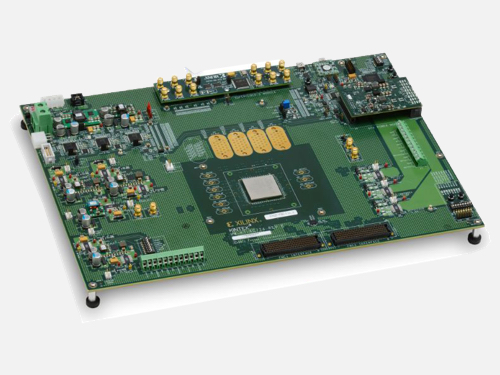
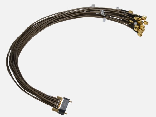
The Kintex®-7 FPGA KC724 Characterization Kit provides the hardware environment for characterizing and evaluating 16 GTX (12.5Gbps) transceivers of the on-board Kintex-7 K325T FPGA. The KC724 allows evaluation of the Integrated Bit Error Ratio Test (IBERT) demonstration using either the Vivado® or ISE® design suites. Each GTX Quad and its associated reference clock are routed from the FPGA to a connector pad which is designed to interface with a Samtec BullsEye connector. A cable enabled with a BullsEye connector and 10 standard SMAs allows users to connect to a broad range of evaluation platforms, from backplanes and optical evaluation boards to high speed test equipment. Each BullsEye connector handles a full GTX Quad, four transmit/receive pairs as well as the two independent reference clocks, enabling the highest level of flexibility in testing custom applications.
Key Features & Benefits
- Hardware environment for characterizing and evaluating 16 GTX (12.5Gbps) transceivers on Kintex-7 FPGAs
- Hardware, design tools, IP, and pre-verified reference designs
- Integrated Bit Error Ratio Test (IBERT) reference design
- Expand I/O with the FPGA Mezzanine Card (FMC) interface
- BullsEye connector supporting a full GTX Quad, with four transmit/receive pairs
- System ACE™ SD controller
- Four Samtec BullsEye connector pads for the GTX transceivers and reference clocks
- Two pairs of differential MRCC inputs with SMA connectors
Featured Xilinx Devices
Featuring the ROHS compliant KC724 kit including the XC7K325T-3FFG900E FPGA
| Logic Cells | 326,080 |
|---|---|
| DSP Slices | 840 |
| Memory (Kb) | 16,020 |
| GTX Transceivers | 16 |
| I/0 Pins | 500 |

Product Information
Board Features
Featuring the Kintex-7 KC724 Evaluation Board

Communication & Networking
- Four Samtec BullsEye connector pads for the GTX transceivers and reference clocks
- Two pairs of differential MRCC inputs with SMA connectors
- USB-to-UART bridge
Clocking
- Fixed, 200 MHz 2.5V LVDS oscillator wired to multi-region clock capable (MRCC) inputs
- SuperClock-2 module supporting multiple frequencies
Display
- Power status LEDs
- General purpose DIP switches, LEDs, push buttons, and test I/O
Expansion Connectors
- Three VITA 57.1 FPGA mezzanine card (FMC) high pin count (HPC) connectors
Configuration
- Digilent USB JTAG programming port
Memory
- System ACE™ SD controller
Control & I/O
- I2C Bus
Power
- PMBus connectivity to on-board digital power supplies
What's Inside
KC724 Evaluation Board
Featuring the Kintex-7 XC7K325T-3FFG900E FPGA
Full seat Vivado® Design Suite: Design Edition
Node locked & Device-locked to the Kintex-7 XC7K325T FPGA, with 1 year of updates
Samtec Bullseye Cable
10 standard SMAs
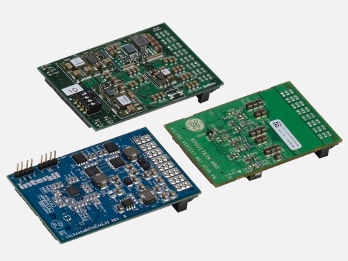
Superclock-2 Module Supporting Multiple Frequencies
Resources
Design Tools
| Name | Description | License Type |
|---|---|---|
| Vivado Design Suite Design Edition | The Xilinx Vivado® Design Suite is a revolutionary IP and System Centric design environment built from the ground up to accelerate the design for FPGAs and SoCs. |
Node locked & Device-locked to the Kintex-7 XC7K325T-3FFG900E FPGA, with 1 year of updates |


