Quality by Design
Xilinx product are designed to meet and operate reliably to their maximum specification. We are an engineering-driven organization focused on advanced technologies, methodologies and tools.
- Overview
- Design for Reliability
- Design for Test
- Design for Manufacturability
- New Product Introduction
- Verification & Characterization
Advanced design and manufacturing technology increasing complexity require rigorous development process to achieve the most stringent quality standards and fuel innovation. These efforts have come together in our new, robust Integrated Platform Development Lifecycle model. The process involves the early planning and architecture of an aligned set of pre-validated elements that are delivered as a complete “design platform” solution to offer optimal performance, the highest quality results, and a superior “out-of-the-box” design experience for devices and boards.
- Better customer-driven product definition
- Stronger and earlier development controls
- Design Tools PRODUCTIVITY, which pushes ease of use to new levels with proven design
- Methodologies, predictable QoR, and significantly improved user experiences
- Enhanced customer design capabilities with software developments and embedded platforms
- Tighter release criteria for engineering samples and fast transition to production
- Leading 16nm product family with 3-Peat (28/20/16nm) in time-to-market
- UltraScale™ architecture for simple migration between planar and FinFET nodes
- First ISO26262 product family certified for robust systematic and random defect management
- Second-generation 3D IC/PS architecture leveraging proven technology
Software Quality
The Vivado® Design Suite along with the Xilinx software development environments (SDx) represent a major advancement in ease of use for Adaptive Computing Accelerator Platform (ACAP) developers. Xilinx development tools accelerate integration, implementation, verification and debug capability, and have been designed to handle exponential growth in device densities reaching 10s of millions of logic cells. In 2019, Xilinx introduced Vitis – Unified software platform for all developers.
Vivado/SDx Quality Initiatives:
- High quality with extensive and continuous daily regression suites with over 220,000 nightly tests
- Weekly regression testing of over 90K interactive, batch, formal checking, directive random and hardware testing
- Robust release checklist and criteria
- ISO26262 functional safety certified since 2016
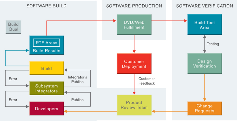
Figure 1. Vivado Quality Initiatives.
Vivado™/SDx IP Quality Initiatives:
- XVI - Xilinx Verification Initiative (Functional Verification) – UVM based methodology
- Viper - Next generation verification across all Vivado IP - 80,000+ IP test jobs per day
- System Level Validation (SLV) - Over 250 different IP tested, over 1500+ systems tested daily
- SEM IP ISO26262 functional safety certified since 2013

Figure 2. Vivado IP Quality Initiatives.
Earlier and more stringent testing and verification mitigate the risks that stem from increasing complexity. Testing with higher-level customer designs increased the prerelease discovery and resolution of issues. With more issues identified during development, the impact on customers is minimized and design cycles are accelerated for higher-quality products and an improved user experience.
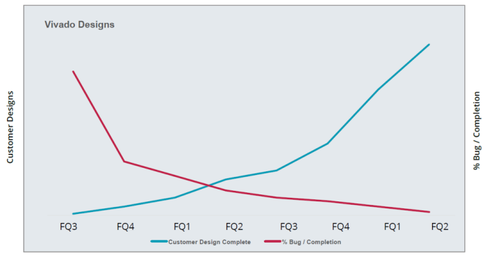
Figure 3. Earlier and more stringent testing and verification mitigate the risks that stem from increasing complexity. Testing with higher-level customer designs increased the prerelease discovery and resolution of issues. With more issues identified during development, the impact on customers is minimized and design cycles are accelerated for higher-quality products and an improved user experience.
Design for Reliability (DFR)
Enhanced Design-for-Reliability (DFR) methodology and guidelines have proven a FIT rate less than 12 at production. Appropriate reliability design rules, budgets and guardbands were established to address post-stress degradations and long-term reliability.
Xilinx reliability methodologies overcame the shrinking reliability margins for the leading process nodes. By leveraging early learning, in-depth tools expertise and machine-learning, Xilinx engineers shortened development processes from months to days, and accommodated the extra iterations required for 28/20/16nm. As a result, Xilinx devices are meeting the stringent requirements of the most reliability-sensitive applications in industrial, automotive, aerospace, and defense industries through:
- Improved outlier elimination and new DFR methodology are combating the “shrinking bathtub” curve
- Xilinx engineering and quality assurance programs have yielded proven, predictable, and very-low failure rates over extended device lifetimes
- The 28/20/16nm devices were released to production with power and defect density (DD) beating previous estimations
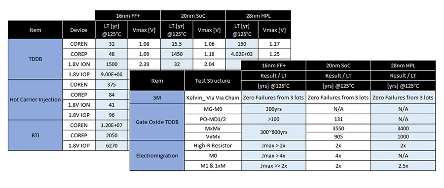
Figure 1. From 28nm to 16nm, wafer-level reliability exceeds transistor and interconnect market requirements to deliver industry-leading device FIT.
Design for Test (DFT)
“If you can’t test it, then don’t design it.” Xilinx design engineers place priority on the ability to detect problems quickly and identify root causes that enable solutions. The Xilinx approach starts with Design-for-Test (DFT) methodologies and the New Product Introduction (NPI) process, and extends throughout the complete product life cycle.
Xilinx continuously improves the test methodology of all products from generation to generation through implementing various Design-for-Testability (DFT) methods and tools. These techniques span digital logic, IP, memory elements, I/O boundary scanning, and many other areas. New test methodologies are measured against PPM results from customer returns. It builds quality into the design of world’s most advanced technology and largest All Programmable / Adaptive Computing Accelerator Platform (ACAP) die.
Design methodology focused on quality integration through all phases of design cycle:
- DFX key features such as PS core LBIST / MBIST / JTAG / ECC / Redundancy
- Validation platforms emulation and sub-system
- Extensive use of test chips to validate key IPs (DDR / SERDES / MC)
- Extensive use of Open Source community for System Software Solutions (PetaLinux)
| Circuit Under Test | Primary Fault Target and Type | Test Methodology | Test Coverage Metric | |
|---|---|---|---|---|
| Type | Example | |||
| Degital Logic | Combinational and Sequential Circuits | Single stuck-at faults | Deterministic ATPG, LBIST and fault-graded functional vectors | Overall entire FPGA > 99%, individual IP blocks range from 98% to 99.9% |
| At-speed transition faults | Deterministic transition ATPG or LBIST | 80-92% depending on IP block | ||
| Path delay faults | Path delay ATPG | First 500 | ||
| IP | High-speed I/Os, e.g., SerDes, and BER DDR | BER | PRBS Ioopback (both near end and far end for SerDes) | 100% industry-standard testing |
| PRBS Ioopback for DDR, embedded BERT, Tx to Rx internal parallel loopback | 100% industry-standard testing | |||
| PLL | Jitter, frequency | Embedded BIST | 100% functional test | |
| Mixed-signal IPs | Analog defects (no digital type of defects) | Functional vectors or functional BIST | 100% functional test | |
| Memory elements | Embedded memory | Cell stuck-at, stuck-open, coupling, transition, address decoder, transient R/W, data retention, and port fault for multiport memory | Mats = algorithm for all port widths: 13n moving inversion algorithm; two-port memory tests; at-speed tests | 100% industry-standard testing |
| I/O boundary scan | Open, short, stuck at | Boundary scan IEEE 1149.1 for all I/Os and IEEE 1149.6 for high-speed I/Os | 100% functional test | |
| Misc. / Other | Temp sensor | Measure on-die temperature | JTAG accessible | 100% functional test |
| Voltage sensor | Measure on-die voltage | JTAG accessible | 100% functional test | |
| Electronic chip ID | Device ID including wafer lot, wafer number, X/Y coordinates | JTAG accessible | 100% functional test | |
Table 1. Key Manufacturing Tests: These test examples illustrate the test methodology innovation and continuous improvements that are intrinsic parts of the Xilinx engineering culture. Learnings from previous generations and excellent coverage are leveraged to overcome the challenges with newer technology and ultimately enable the release of high-quality Adaptive Computing Accelerator Platforms (ACAPs).
Design for Manufacturability (DFM)
Xilinx Design-for-Manufacturability (DFM) engineering discipline ensures quality, reliability, and time-to-market by focusing on mitigating risks and optimizing operational excellence. It starts with rigorous design of experiments, tests and manufacturing methodologies such as:
- DFM rules that provide performance advantages
- Modular design and reuse with technology risk proofing & mitigation
- Characterizing devices more deeply using advanced tools & methods
- Reliability prediction, using a custom-hierarchical, end-to-end tool that draws on a Xilinx design database
- Expanded wafer qualification using three additional elements for assembly testing: electrical, thermal, and mechanical
- Ensuring multiple-die performance by adding system-timing checks to characterization process
- Enabling power die optimization during selection, through fully-integrated die-testing at wafer sort, now standard across the 7-series, UltraScale, and UltraScale+™
- Collecting more data to prove operational performance & software models
These methodologies behind the industry’s first 28nm (28Gb/s) 3D IC heterogeneous devices and now extended at 20nm (33Gb/s) and 16nm (56Gb/s) – Figures 1 and 2 – are fully integrated to meet performance and specifications.
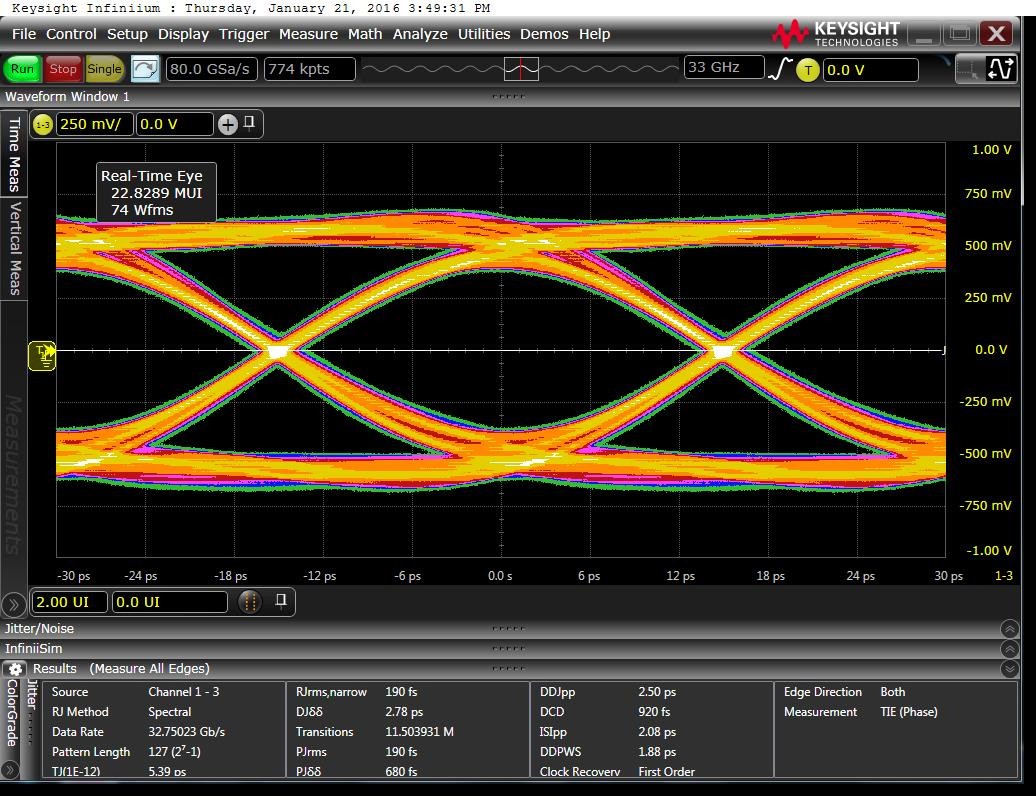
Figure 1. 33Gb/s Eye Diagram in 20nm
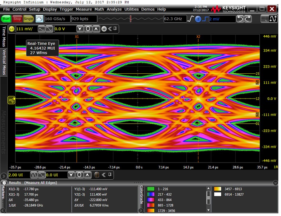
Figure 2. 56Gb/s Eye Diagram using PAM-4 in 16nm
New Product Introduction (NPI) Process
Xilinx New Product Introduction (NPI) process was established and refined over the last five generations of Xilinx technology, culminating in our 28/20/16nm products, which include our FPGAs, 3D ICs and SoCs devices. The NPI is a robust and rigorous process with stringent exit criteria targeting the highest quality of Xilinx products in Engineering Silicon (ES) and production release phases. Learn more about how Xilinx delivered a generation ahead at 28nm and is staying a generation ahead at 20nm and 16nm. Some NPI activities include:
- Performance validation over process corners, to check for margin over PVT for manufacturability
- Comprehensive attributes, with sweeps above and below default settings to confirm margin and highlight sensitivities to PVT, with higher focus on applicable MGT, BRAM, and MMCM
- Improved dynamic power characterization to better isolate specific power blocks, with extensive validation of Xilinx Power Estimator (XPE) and Xilinx Power Analyzer (XPA) models over toggle rates and PVT
- NPI process integration with product life cycle

Figure 1: From first silicon to production material ship, Xilinx has redefined its verification and characterization process to drive early discovery to release with zero errata.
The results are in and have ended all debate. The company embraced a hallmark zero-defect mentality with focus on quality and reliability-which spans across design, process development, assembly, and test-guided by fifth-generation new product introduction (NPI) processes and the most stringent release criteria to date.
The end-result of Xilinx commitment to quality is exhibited with Customer Quality Scorecards, a direct feedback mechanism provided by our customers. With all the challenges related to shrinking process nodes, DFT, DFR and DFM expectations keep increasing to sustain the excellent results, demonstrated by customer-experienced PPM results.
Verification and Characterization (V&C)
Xilinx Verification & Characterization (V&C) ensures that products operate over the specified voltage and temperature ranges. V&C starts with building in sufficient margin in the design phase, which is then validated during simulation prior to product tape out. Critical circuits are verified using test vehicles. Finally, production-ready product quality is characterized based on the datasheet and Xilinx IP across all process corners, voltage, and temperature (PVT) combinations. The data is used to evaluate product performance against the published datasheet and established production test margins.
Xilinx engineers have proven that they verify, characterize, test, and qualify devices better and faster than anyone else in the industry. At 16nm, the advancements improved data collection, verification, and characterization with:
- Highly automated design flows and timing analysis
- Verification and Characterization (V&C) process for earlier identification of issues using earlier corner material
- Known-good die testing at wafer sort, which is critical due to 3D slice density and yield
- Die selection, power die optimization, and performance to address the most stringent requirements (power vs. performance)
- Test methodologies for processor subsystem (PSS) and FPGA interaction, to meet performance, specification, and quality requirements
- Expanded data collection and test cases for verification and characterization (including system-level test)
- Joint-safe-launch quality at the system-level for advanced systems and packaging to track more advanced applications, with system-level testing being a significant component in the Xilinx Volume-System-Testing (VST) over 10,000 devices to emulate customer use cases

Figure 1. SSO Data: With package complexity, SSO characterization data validates Xilinx simulation methodologies that contribute to packaging design.
With every product release, Xilinx publishes characterization reports that validate product datasheet specifications and give customers a better understanding of Xilinx methodologies and techniques. The following steps depict the key milestone criteria prior to release of characterization reports and product specifications:
- Test patterns for all blocks, during both automated and bench testing
- Full-functionality verification across speed, process, and temperature
- Power and performance verifications, corner cases, and system testing
- Volume automated-test-equipment (ATE) characterization

Figure 2. Sample Characterization Report: With every product release, Xilinx publishes characterization reports that validate product datasheet specifications and give customers a better understanding of Xilinx methodologies and techniques.


