AR# 35193
|MIG Virtex-6 DDR2/DDR3 - Debugging Read Leveling Stage 2
描述
This Answer Record details items that should be analyzed to verify Read Leveling Stage 2 of the MIG Virtex-6 DDR2/DDR3 calibration process completed as intended. For general information on the Read Leveling Stage 2 calibration process, see (Xilinx Answer 35129).
NOTE: This Answer Record is contained in a series of MIG hardware debug Answer Records and assumes you are running the MIG Example Design with the Debug Port Enabled. It is best to start at the beginning of this recommended debug flow. Please see (Xilinx Answer 34588) to start from the beginning of the hardware debug flow.
NOTE: This Answer Record is part of the Xilinx MIG Solution Center (Xilinx Answer 34243). The Xilinx MIG Solution Center is available to address all questions related to MIG. Whether you are starting a new design with MIG or troubleshooting a problem, use the MIG Solution Center to guide you to the right information.
解决方案
Signals of Interest:- Calibration State machine variables (useful ChipScope trigger)
- cal2_state_r = Stage 2 state machine
- Byte Count (useful Chipscope trigger)
- cal2_cnt_rden_r = Stage 2 byte being calibrated
- Bitslip Count
- dbg_rd_bitslip_cnt = Number of bit times data is delayed
- Read Clock Delay Count
- dbg_rd_clkdly_cnt = Number of bit times data is delayed
- Write Clock Delay Count
- dbg_wr_calib_clk_delay[1:0] = Number of clock cycles to delay writes internally to account for write-leveling skew/DQS inversion
- Read command to data count
- dbg_rd_active_dly = Number of clock cycles after a read command is issued that data returns
- Read Data to verify data pattern
- dbg_data = Data read back. Divide data bus by 4 and data can be grouped as rd_data_rise0, rd_data_fall0, rd_data_rise1, rd_data_fall1. For example, dbg_rddata[63:0] : [15:0] = rise data 0 , [31:16] = fall data 0, [47:32] = rise data 1, [63:48] = fall data 1
The Read Leveling logic is contained in the 'rtl/phy/phy_rdlvl.v/.vhd' module.
Debug Steps:
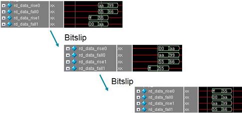
During Stage 2, the data pattern "FF00AA5555AA9966" is continuously written and readback. The writes are shifted while for reads bitslip and alignment occurs. This performs not only Write Calibration to align the DQS Group to the correct CK cycle, but also Read Leveling Stage 2 which aligns the captured data word in the resynchronization clock domain.
- Analyze the read data using ChipScope to see the shifting occur. Following is a pictorial view of the shift to alignment:
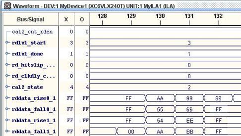
- Verify the read data pattern read back is accurate and aligned. This means the pattern (FF00AA5555AA9966) is captured starting on rddata_rise0. The below ChipScope waveform shows an incorrect data pattern readback with incorrect alignment.
In this waveform, the data pattern is incorrect. It should be FF00AA5555AA9966 starting on rddata_rise0. Instead, the pattern starts on rddata_rise1 and includes a 54 instead of 55. This shows that not only is the pattern incorrect, but bitslip did not complete successfully. Successful completion of bitslip results in aligned data starting on rddata_rise0. See below for possible reasons the data pattern is incorrect.
How to tell which byte is failing during stage 2 calibration?
- Observe dbg_wr_calib_clk_delay. This bus includes 2 bits for each DQS Group. Whenever each group of 2 bits equals a value of 3, the corresponding byte failed calibration. For example, if bits [1:0] = 3, then byte[0] is not calibrated.
What can go wrong?
- Stuck at bits (or unconnected bits on PCB)
- Unmatched traces
- Marginal Signal Integrity Issue
- Ensure SI Simulations using IBIS are performed
- Wrong Pin-out
- Moving bytes to another column without adjusting certain parameters in the RTL.
- Problems with the write of calibration data.
- For information on isolating a read versus a write error, please see (Xilinx Answer 35209).
- Pin-Out/Banking Requirements (Xilinx Answer 34308)
- Board Layout Requirements (Xilinx Answer 34544)

