AR# 34533
|Design Advisory for Spartan-6 FPGA Block RAM - Address Space Overlap
描述
Under certain conditions, in which addresses overlap, it is possible that the contents of the Spartan-6 FPGA block RAM can become corrupted. This Answer Record provides additional details to that found on page 15 of the Spartan-6 FPGA Block RAM User Guide (UG383), which also includes other conflict avoidance descriptions.解决方案
Issue Description:Under certain conditions it is possible that the contents of the Spartan-6 FPGA Block RAM can become corrupted.
The issue only occurs when using Read First mode with either of the following setups with different clocks clocking CLKA and CLKB of the Block RAM:
- True Dual Port (TDP) mode with WRITE_MODE = READ_FIRST for the RAMB16BWER or RAMB8BWER components
- Simple Dual Port (SDP) mode with WRITE_MODE = READ_FIRST for the RAMB8BWER component
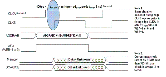
When a write operation is performed and a subsequent read operation of the other port is attempted on one of the overlapping addresses, the read operation might fail and the contents of the memory locations being accessed can become corrupted. If CLKA and CLKB of the Block RAM are driven by the same clock, no collision will occur and read and write operations will succeed with no memory corruption. Please see the figure and table below for further details on what clocking schemes will be affected by this issue, and review the "Workaround" section for ways to work around the issue.
Figure 1:

Table 1: Address Collision Conditions
| RAMB16 Primitive | RAMB8 Primitive | |
| Address Collision | When both ports are enabled (ENA and ENB =1 ), not using the same clock on both ports (CLKA CLKB), the phase offset between clocks can never be between 100 ps and 3 ns (or the next clock edge) and one of the following: 1) Both port widths are 18 and under: A13-A6,A4 are the same on both ports 2) The port width is 36 on either or both ports: A13-A7, A5 are the same on both ports. |
When both ports are enabled (ENA and ENB = 1) and not using the same clock on both ports (CLKA CLKB) and A12-A6, A4 are the same on both ports |
| No Address Collision | When either port is disabled (ENA or ENB = 0), using the same clock on both ports (CLKA == CLKB), the phase offset between clocks is never between 100 ps and 3 ns (or the next clock edge) or one of the addresses in the following cases is always different for the two ports 1) Both port widths are 18 or under: A13-A6,A4 2) The port width is 36 on either or both ports: A13-A7,A5 |
|
Affected Components:
- RAMB16BWER or RAMB8BWER in TDP mode with WRITE_MODE set to READ_FIRST on either port.
- RAMB8BWER in SDP mode with WRITE_MODE set to READ_FIRST.
- All UNIMacro components with WRITE mode set to READ_FIRST on either port.
Behavior in Software:
- ISE 12.3 and later - the software has been updated to include SDP Write First Mode as the preferred workaround to the Address Overlap issue. In SDP Write First Mode, address overlap may occur, but it would only result in a failed read, and not a corruption of the memory cell(s). See the Work-around section for more details.
- In ISE 12.1 and 12.2 -the result of simulation does illustrate the problem to the user. The simulation models have been updated to alert the user about this condition and will reflect unknowns where corruption could occur.
- In ISE 11.5 and earlier -the result of simulation does not illustrate the problem to the user. Simulation behavior will look normal and no error or warning will be generated. Hardware can, however, exhibit functional failures in the form of memory array and/or read corruption.
Workaround:
- Starting in ISE 12.3 software, WRITE_FIRST mode is supported for Simple Dual Port (SDP) Block RAM, and is the preferred workaround.
- For all SDP Block RAM with RDCLK and WRCLK driven by the same clock, use READ_FIRST mode, since no collision will occur in this case. If RDCLK and WRCLK of a SDP Block RAM are driven by different clocks, use WRITE_FIRST mode. In WRITE_FIRST mode, users must design around the conflict avoidance requirement that exists when one port performs a write operation and the other port simultaneously reads from the same location.
- CoreGenerator IP and XST have been updated to support the WRITE_FIRST mode feature. If using the Block RAM Generator to generate Simple Dual Port configurations of Block RAM, select and generate v4.3 of the core to use WRITE_FIRST mode.FIFO Generator v6.3 automatically uses WRITE_FIRST Simple Dual port Block RAM when necessary.
- To enable WRITE_FIRST mode for SDP Block RAM, add the following two constraints on all desired Block RAM in the UCF file:
- INSTWRITE_MODE_A=WRITE_FIRST;
- INSTWRITE_MODE_B=WRITE_FIRST;
- For True Dual Port (TDP) modes, determine if READ_FIRST mode is absolutely necessary. If not, use WRITE_FIRST or NO_CHANGE modes.
- Perform a full timing simulation under all conditions with the updated simulation model when it becomes available in the ISE 12.1 software. At minimum, post-synthesis simulation should be run in order to identify any potential collisions.
本答复记录是否对您有帮助?