AR# 30915
|Virtex-5 GTP RocketIO - MGTAVCC Power recommendations for unused tiles between calibration resistor and instantiated tiles
描述
The GTP Transceivers in the Virtex-5 LXT and SXT FPGAs use a calibration circuit to accurately determine the termination resistance for all transceivers in a column. This circuit is located in bank 112 for each device and utilizes a single reference resistor connected to MGTTREF_112. To correctly power this circuit and allow propagation of the calibration information to instantiated GTP_DUAL tiles, certain power guidelines must be followed.解决方案
Bank 112
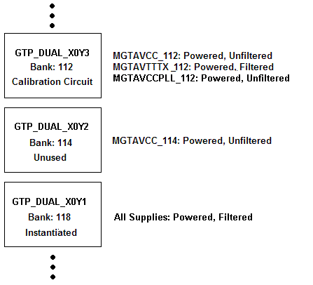
The calibration circuitry for the entire column is connected to this tile and, in addition to MGTAVTTRXC, is powered from MGTAVTTTX, MGTAVCCPLL and MGTAVCC. All three of these supplies must be powered while only MGTAVTTTX must be filtered per Table 25 in the Virtex-5 FPGA Data Sheet, DS202:
http://www.xilinx.com/support/documentation/data_sheets/ds202.pdf
Unused tiles between bank 112 and those instantiated in a design
Each unused tile between bank 112 and a GTP_DUAL instantiated in a design must be MGTAVCC powered. For example, in a Virtex-5 LX50T in an FF665 package GTP_DUAL_X0Y3 is bank 112 and contains the calibration circuitry. If GTP_DUAL_X0Y1 is the only tile used in the design, GTP_DUAL_X0Y2 must still be supplied MGTAVCC. For these intermediate tiles, MGTAVCC does not require the filtering otherwise necessary.

Relative Locations of GTP tiles
GTP locations are sequential, with X0Y0 starting at the bottom of the device and counting up to X0Yn. Locations can be correlated to a particular bank by referring to the Package Placement Information section of the Virtex-5 FPGA RocketIO GTP Transceiver User Guide:
http://www.xilinx.com/support/documentation/user_guides/ug196.pdf